2.1SPI interface
The two controllers communicate with the sbRIO with two separate SPI buses that can run at clock rates of up to 18MHz. The microcontrollers are configured as slaves. They can activate an interrupt line in order to force FPGA of sbRIO (which is master) to retrieve microcontroller data. The data size is always 16 bit (referenced as one word).
2.1.1Transmission protocol
The following communication protocol is used for communication in both directions (FPGA to microcontroller, microcontroller to FPGA).
| Word | Name | Range/value |
|---|---|---|
| 0 | LEN (number of data words) N | 1…65535 |
| 1 (high byte) | SIGNATURE | always 0x4D |
| 1 (low byte) | CRC8 (of all following data bytes) | 0x00…0xFF |
| 2 (high byte) | COMMAND | 0x00…0xFF |
| 2 (low byte) | DATA (byte 0) | 0x00…0xFF |
| … | … | … |
| 2+N-1 (low byte) | DATA (byte N-1) | 0x00…0xFF |
It must be noticed that only the low byte of the data area is used. The high byte always contains the constant 0x40 for data messages (except data word 0, which contains the command byte additionally) or 0x80 for status messages (compatibility reasons, FPGA discards received data words with a value less or equal to 0x00FF). A data word with a value of 0x0000 will be added automatically by the microcontroller in order to clear its SPI buffer.
2.1.2Status codes
Each command received from sbRIO will be answered by the microcontroller. This can be done by a data message (which contains application data processed by RT/PC) or a status message. It is possible to deactivate this functionality by command.
The following status codes are defined.
| Value | Content |
|---|---|
0x01 | ACK (command processed successfully, but no data bytes to send for response) |
0x02 | PAR (at least one parameter is out of range) |
0x04 | CMD (command not known) |
0x08 | IDX (object index out of range) |
0x10 | CRC (checksum verification failed) |
0x20 | SIG (wrong signature read) |
0x40 | TIM (SPI timeout detected) |
0x80 | LEN (command length mismatching) |
2.1.3Command description
The latest descriptions can be found in the VI documentation.
2.2Non-volatile storage of data
The on-board data flash of the two STM32 can be used as an EEPROM for the non-volatile storage of data (for example baud rates, ID filter settings, termination resistances …).
2.3Analog Input
The interface of the analog input board consists of
- 3 address buses for multiplexing the analog channels for every analog group separately
- Signals for the serial communication with the ADCs.
- Serial interface to the EEPROM for calibration data.
2.3.1Multiplexers
As shown in the functional block diagram, the channels are multiplexed to ADCs with two channels each. 32 single-ended channels are handled by a 32:1 multiplexer with address lines ADR1_0 to ADR1_4, the remaining 16 single-ended channels are handled by a 16:1 multiplexer with address lines ADR2_0 to ADR2_3 and the differential channels are switched using two 8:1 multiplexers with shared address lines ADR3_0 to ADR3_2.
All address lines are buffered using high-speed CMOS buffers to reduce the load for the FPGA output drivers and to provide clean signals on the PCB.
The address lines are switched during the ADC hold phase to avoid influencing the conversion results.
The inputs are sampled by the internal Sample & Hold stage of the ADCs between the 32nd rising edge of SCK and the rising edge of CONV.
2.3.2ADCs
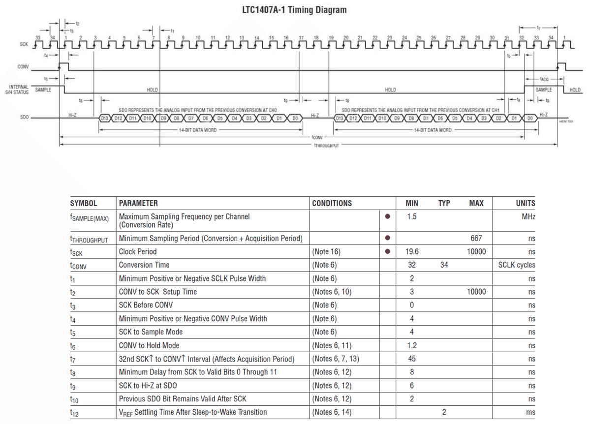
Both ADCs are clocked by the same CONV and SCK signals.
The ADC outputs are buffered using high-speed CMOS buffers to drive the ribbon cable’s capacitance.
2.3.3EEPROM
The EEPROM contains an ID to identify the PCB as an analog measurement card, the type (128 or 64 channel version), a calibration timestamp and the hardware version. Furthermore offset and gain calibration data for each channel is stored as well as the input voltage scaling factor according to the resistor dividers on the PCB. There is an EEPROM present for every analog subsystem respectively. Following table shows an excerpt of the EEPROM content. A detailed memory map can be found in the separate file “EEPROM Memory Map Analog_LDSA.xlsx”.
| Address | Content | Values | Comment |
|---|---|---|---|
| 0 | ID | 0xAA | Identifies the PCB as analog measurement card |
| 1 | Hardware revision | e.g. 0x14 | Hardware revision: e.g. Version 1.3 => 0x13 |
| 2 | Hardware revision: e.g. Version 1.3 => 0x13 | ||
| 3 | Calibration timestamp upper byte | 0x02 | Date of last calibration: e.g. 16.08.2010 => 160810 = 0x2742A |
| 4 | Calibration timestamp middle byte | 0x74 | Date of last calibration: e.g. 16.08.2010 => 160810 = 0x2742A |
| 5 | Calibration timestamp lower byte | 0x2A | Date of last calibration: e.g. 16.08.2010 => 160810 = 0x2742A |
| 6 | |||
| 7 | |||
| 8 | |||
| 9 | Offset byte 1 single-ended channel 1 | Bit31…24 | Offset in Steps of µV |
| 10 | Offset byte 2 single-ended channel 1 | Bit23…16 | Offset in Steps of µV |
| 11 | Offset byte 3 single-ended channel 1 | Bit15…8 | Offset in Steps of µV |
| 12 | Offset byte 4 single-ended channel 1 | Bit7…0 | Offset in Steps of µV |
| 13 | Gain byte 1 single-ended channel 1 | Bit31…24 | Gain of input voltage divider multiplied by 109 |
| 14 | Gain byte 2 single-ended channel 1 | Bit23…16 | Gain of input voltage divider multiplied by 109 |
| 15 | Gain byte 3 single-ended channel 1 | Bit15…8 | Gain of input voltage divider multiplied by 109 |
| 16 | Gain byte 4 single-ended channel 1 | Bit7…0 | Gain of input voltage divider multiplied by 109 |
| 17 | Offset byte 1 single-ended channel 2 | Bit31…24 | Offset in Steps of µV |
| 18 | Offset byte 2 single-ended channel 2 | Bit23…16 | Offset in Steps of µV |
| 19 | Offset byte 3 single-ended channel 2 | Bit15…8 | Offset in Steps of µV |
| 20 | Offset byte 4 single-ended channel 2 | Bit7…0 | Offset in Steps of µV |
| 21 | Gain byte 1 single-ended channel 2 | Bit31…24 | Gain of input voltage divider multiplied by 109 |
| 22 | Gain byte 2 single-ended channel 2 | Bit23…16 | Gain of input voltage divider multiplied by 109 |
| 23 | Gain byte 3 single-ended channel 2 | Bit15…8 | Gain of input voltage divider multiplied by 109 |
| 24 | Gain byte 4 single-ended channel 2 | Bit7…0 | Gain of input voltage divider multiplied by 109 |
| : | : | : | |
| : | : | : | |
| 511 | Gain byte 3 differential channel 15 | Bit15…8 | Gain of input voltage divider multiplied by 109 |
| 512 | Gain byte 4 differential channel 15 | Bit7…0 | Gain of input voltage divider multiplied by 109 |
| 513 | Offset byte 1 differential channel 16 | Bit31…24 | Offset in Steps of µV |
| 514 | Offset byte 2 differential channel 16 | Bit23…16 | Offset in Steps of µV |
| 515 | Offset byte 3 differential channel 16 | Bit15…8 | Offset in Steps of µV |
| 516 | Offset byte 4 differential channel 16 | Bit7…0 | Offset in Steps of µV |
| 517 | Gain byte 1 differential channel 16 | Bit31…24 | Gain of input voltage divider multiplied by 109 |
| 518 | Gain byte 2 differential channel 16 | Bit23…16 | Gain of input voltage divider multiplied by 109 |
| 519 | Gain byte 3 differential channel 16 | Bit15…8 | Gain of input voltage divider multiplied by 109 |
| 520 | Gain byte 4 differential channel 16 | Bit7…0 | Gain of input voltage divider multiplied by 109 |
2.4Digital output
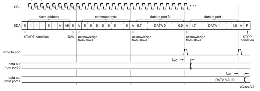
As shown in the block diagram, the relays can be accessed via two I²C port expanders. All pins are configured as inputs at power-up and must be reconfigured as outputs before the relays can be switched.
Addresses for write access:
- Port expander 1 (relays 01 to 15):
0b11101000=0xE8 - Port expander 2 (relays 16 to 32):
0b11101100=0xEC - Port expander 3 (relays 33 to 48):
0b11101110=0xEE - Port expander 4 (relays 49 to 64):
0b11101010=0xEA
The LSB is set to zero for write access.
Write to output ports:
Write to configuration registers:

Documents and downloads
Further documents and files for your IRS product are available on myIRS.