1.1Block Diagram
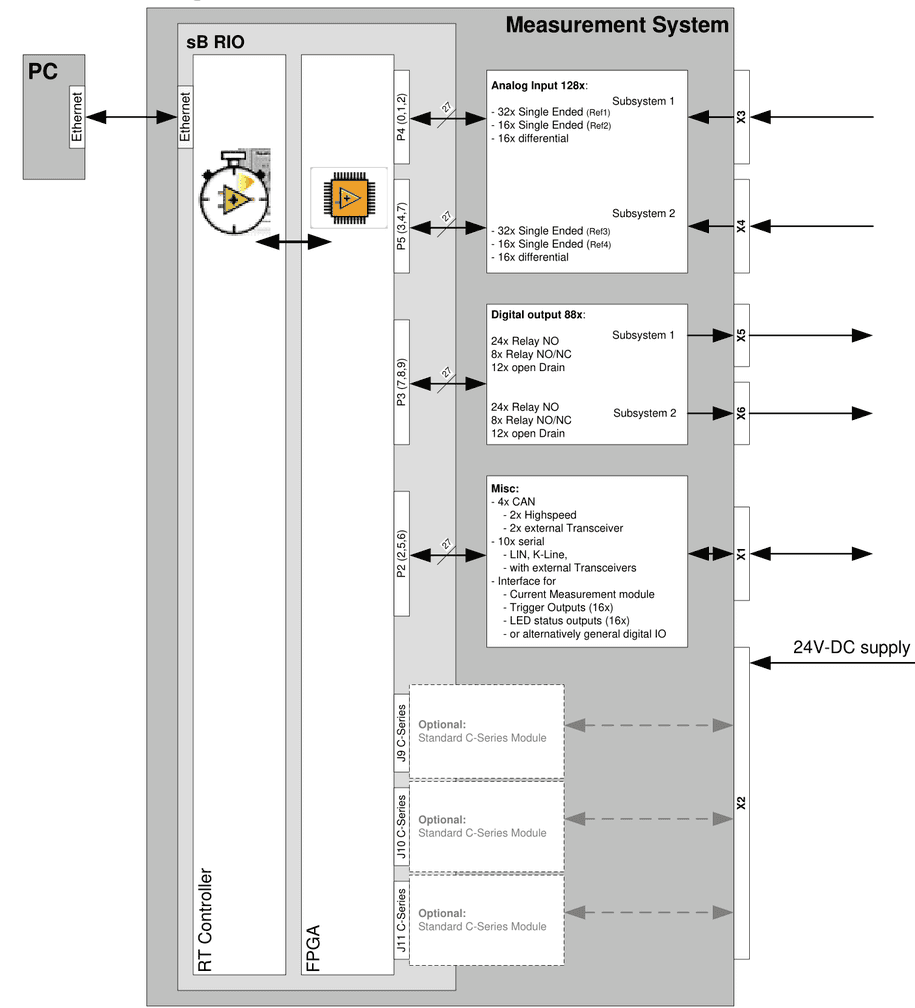
The Measurement system contains the following:
- NI Single-board-RIO sbRIO-9602 (COTS from National Instruments) including
- Processor with real-time Software (LabVIEW RT)
- FPGA for accessing other boards via digital IO and data processing (LabVIEW FPGA)
- 128x Analog inputs with the following configuration twice:
- 32 channels single ended (0…32V / 14Bit)
- 3kS/s parallel / 1,2MS/s single channel
- referenced to a GND node
- 16 channels single ended (0…32V / 14Bit )
- 6kS/s parallel / 1,2MS/s single channel
- referenced to an additional GND node
- 16 channels differential (+-48V / 14 Bit )
- 150kS/s parallel / 1,2MS/s single channel
- 32 channels single ended (0…32V / 14Bit)
- 88x digital outputs with the following configuration twice:
- 24 relays shutters
- 8 relays changeover
- 10 FET outputs referenced to system GND
- 2 FET outputs isolated for any reference GND
- 4x CAN
- 2x high speed with selectable termination resistor (None, 120 Ohm, 60 Ohm)
- 2x without transceiver to implement DUT specific Transceiver in the load-box for high speed, low speed, or special CAN (e.g. E-CAN for trucks)
- 10x serial
- without transceiver to implement DUT specific Transceiver in the load-box for K-Line, LIN, …
- LVDS interface (3x Out, 2x In) for up to 6 cascaded current measurement modules
- 16x open collector output for controlling status LEDs or general purpose output
- 6x digital input for high speed digital signal capturing
- 16x digital IO for low speed digital signal capturing or generation
1.2Power Supply
The Measurement system needs a single 24V DC supply at a current consumption of approx. 700mA in average, 1500mA maximum.
1.3Internal Interfaces
In the standard configuration the measurement system consists of an aluminium carrier which contains 4 printed circuit boards. These are:
- NI Single board RIO board sbRIO-9602 (COTS from National Instruments)
- Base and communication–board (board developed by IRS)
- Digital output board (board developed by IRS)
- Analogue Input board (board developed by IRS)
The following figure illustrates the 4 boards inside the measurement system
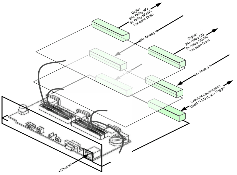
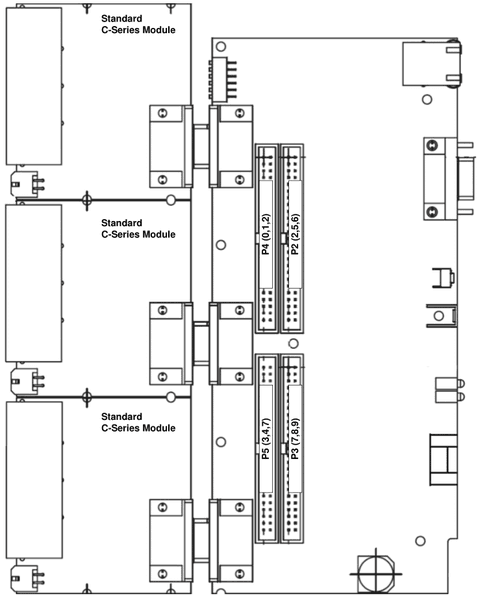
The boards are connected with ribbon cables to the headers P2, P3, P4, and P5 of the sbRIO device. Additionally up to three Compact-RIO c-Series modules can be attached according to the following picture.
For accessing the c-Series external signals the c-Series signals can be routed to a spare 96 pol. connector (DIN41612) on the base and communication board.
1.4External Interfaces
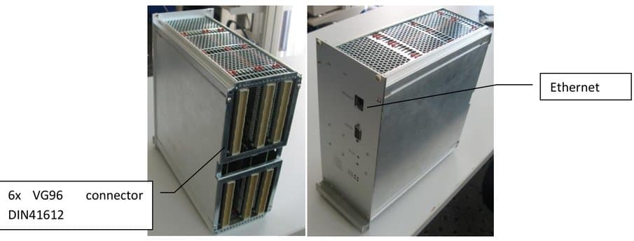
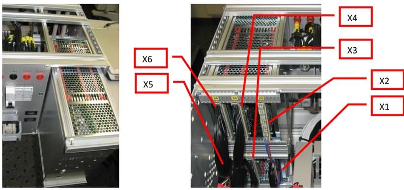
All external connections to the DUT and the load-box are established via 6x 96pol. VG connectors (DIN41612). I.e. the carrier can be plugged into the load-box without any other cabling. The connection for communication with the PC is the only additional cable, which is actually a common Ethernet connection with a standard Ethernet cable.
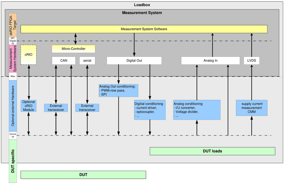
The following block diagram shows a typical setup of the measurement system within a lifetime tester, where additional signal conditioning can be applied for non-standard voltage ranges, load current measurements, analogue outputs, and communication transceivers.
1.5Load box design
The following figure illustrates the typical placement of the measurement system inside the load box from the side view:
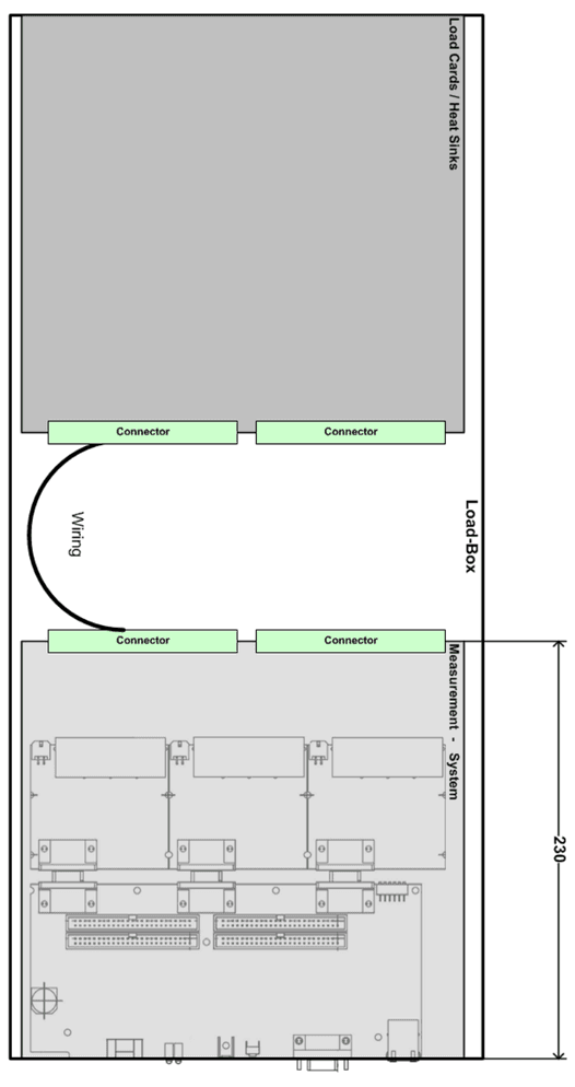
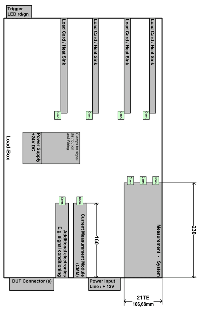
In the typical application of the measurement system the artificial and original loads of the DUT are placed in the front area of the load-box, mounted on heat sinks or other load cards. At the backside the measurement system should be placed with additional electronics like current measurement module, and the connectors to DUT and power supply.
The following figure illustrates the typical placement of the measurement system inside the load box from the top view:
The following figure illustrates the typical placement of the measurement system inside the load box from the top view:
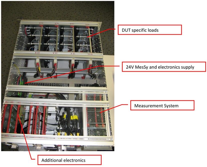
As illustrated in the following figures the measurement system can be plugged into the DUT specific load box
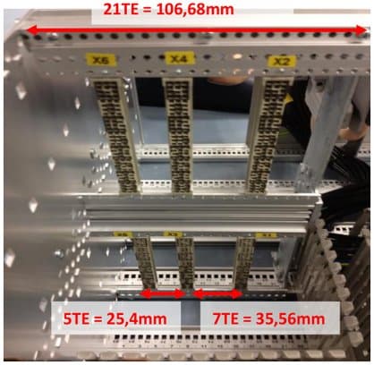
Following figure shows the alignment and dimensions of the VG-Connectors, where the correct placement may be found by counting “holes” on the mounting rail:
1.6GND Concept
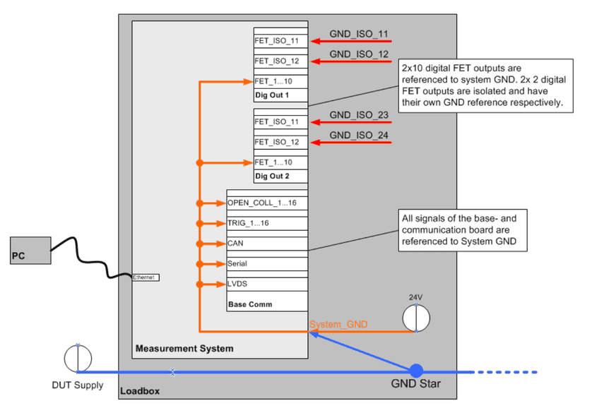
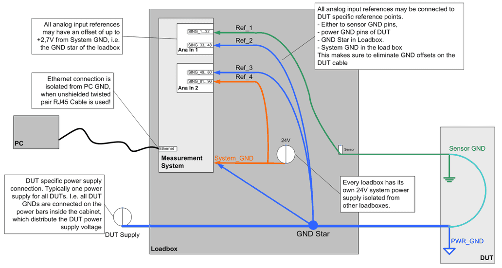
One important issue is the GND concept, when running lifetime testers. MesSy provides a system GND, to which all internal signals and nearly all digital user channels refer to. For analog measurements additional GND reference inputs are available.
1.6.1Digital GND references
Nearly all digital signals are referenced to System-GND, which is determined by the 24V power supply. Voltage drops are usually less problematic for digital signals, but they should be taken into account.
Following figure illustrates the GND concept of the MesSy and its digital channels:
1.6.2Analog GND references for measurement
The GND references for analog measurements are an important issue, since voltages may vary due to voltage drop on the wiring harness. Because of this, analog inputs may be referenced to different voltage levels. These signal levels may vary up to 2,7V over the MesSy system GND, determined by the 24V power supply.
Different reference inputs may also be used to reference the voltage measurements to different DUTs or different GND Pins of one or more DUTs.
Note, that for differential inputs the reference inputs are not relevant, since every channel has its own reference.
1.7Base and communication board
The base and communication card was designed as a carrier and communication board for the sbRIO. Apart from the supply and mounting holes for the sbRIO, it provides
- a total of four CAN channels, with transceiver enable
- up to 10 serial interfaces, with transceiver enable
- 16 open-collector outputs,
- 16 TTL- and CMOS compatible general-purpose IOs,
- three LVDS outputs and two LVDS inputs for communication with the current measurement modules
- I²C interface for external electronic modules.
- 3 slots for extensions with NI Compact-RIO c-Series modules
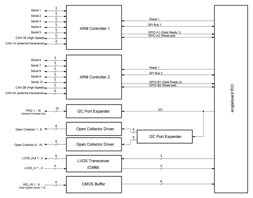
Two microcontrollers with ARM Cortex M3 core are used to provide CAN and serial interfaces; both are used in identical circuits and have separate communication busses as well as separate reset signals to the sbRIO. Deep FIFO buffers for transmission and reception on each interface make sure that no data is lost even when all interfaces are heavily used simultaneously.
1.7.1Block Diagram
1.7.2Specifications
| Item | Min | Typical | Max | Unit |
|---|---|---|---|---|
| Supply current including sbRIO @24V (without additional c-Series modules) | 160 | 240 | 300 | mA |
| Supply Voltage | 20 | 24 | 28 | VDC |
| Number of CAN channels | 4 | |||
| Number of serial interfaces | 10 | |||
| Number of open-collector outputs | 16 | |||
| Number of general-purpose low speed IOs | 16 | |||
| Number of LVDS inputs | 2 | |||
| Number of LVDS outputs | 3 | |||
| Number of general-purpose high speed inputs | 6 | |||
| Number of reserved microcontroller ports | 4 | |||
| Number of reserved c-Series slots | 3 |
CAN communication
For CAN communication there are 4 CAN channels on the board, distributed on two microcontrollers. One CAN channel of each controller is configured as high-speed and offers software-configurable termination (open/120 Ohm/60 Ohm) by means of reed relays. The other channel has to be connected externally to high- or low-speed transceivers with corresponding termination.
| Item | Min | Typical | Max | Unit |
|---|---|---|---|---|
| Supported baud rates | 125 | 1000 | kBit/s | |
| CAN V2.0 High-Speed channels | 2 | |||
| Configurable (high/low-speed) channels | 2 | |||
| Channels with configurable termination | 2 | |||
| Selectable Termination resistance | 60 | 120 | Open | Ohm |
Serial and CAN communication lines with external transceivers
For each of the serial interfaces, three pins are connected to the VG connector: RX, TX and Enable. This allows the external connection of transceiver ICs (RS232, LIN, K-Line, discrete level converters) which can be deactivated using the enable signal. All serial interface and CAN signals for external transceivers meet the following specification
| Item | Min | Typical | Max | Unit |
|---|---|---|---|---|
| Input Low Voltage | -0,5 | 0,4 | V | |
| Input High Voltage | 2,4 | 3,3 | V | |
| Input Current -0,5V < VIn < 3,3V | -1 | +1 | µA | |
| Input Resistance VIn >3,3V or VIn <-0,5V | 220 | Ohm | ||
| Max Output Low Current @VLow < 0,5V | 0 | 1 | mA | |
| Max Output High Current @VHigh > 2,0V | 0 | 1 | mA |
General Purpose IOs Trig 1…16
16 general purpose IOs are available via an I2C port expander. All IOs are protected with series resistors of 220 Ohm. The interrupt pin of the port expander is connected to the sbRIO to allow fast reaction to changing inputs. The general-purpose IOs are provided via an I²C port expander.
| Item | Min | Typical | Max | Unit |
|---|---|---|---|---|
| Input Low Voltage | -0,5 | 1,5 | V | |
| Input High Voltage | 3,5 | 5,5 | V | |
| Input Current -0,5V < VIn < 5,5V | -1 | +1 | µA | |
| Input Resistance VIn >5,5V or VIn <-0,5V | 220 | Ohm | ||
| Max Output Low Current @VLow < 0,5V | 0 | 8 | mA | |
| Max Output High Current @VHigh > 4,0V | 0 | 8 | mA |
Open Collector Outputs 1…16
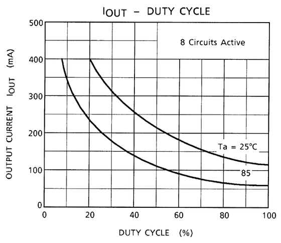
The open-collector outputs can sink currents up to 400mA each, limited by the maximum current carrying capacity of the copper traces.
| Item | Min | Typical | Max | Unit |
|---|---|---|---|---|
| Collector Current per Channel | 0 | 400 | mA | |
| Collector Current for 8 channels all over | See figure below |
If more than one pin per driver IC is used, the maximum allowable current decreases. The figure below shows the de-rating curve if all outputs are used: at 25°C, 125mA per pin are allowed, at 85°C about 60mA.
LVDS Interface for CMM
There are three TX lines and two RX lines available for interfacing with LVDS devices like the Current measurement module CMM_II. The copper traces have been routed with a differential impedance of approximately 100 Ohm and the RX lines are terminated with 100 Ohm resistors.
The copper traces have a width of 350µm and a thickness of 35µm. For epsilonr=4.2 and 475µm prepreg height, the characteristic impedance of a single trace is about 80 Ohm. A differentially routed pair of these traces with a distance of 150µm has a differential impedance of 103 Ohm.
| Item | Min | Typical | Max | Unit | |
|---|---|---|---|---|---|
| LVDS Input | voltage range | -0.2 | 2.7 | V | |
| LVDS Input | Termination | 100 | Ohm | ||
| LVDS Input | Differential input voltage range | 100 | 350 | 600 | mV |
| LVDS Input | Common mode input voltage range | 0.3 | 1.2 | 2.2 | V |
| LVDS Output | Differential output voltage range | 247 | 350 | 600 | mV |
| LVDS Output | Common mode output voltage range | 1.125 | 1.25 | 1.375 | V |
| Typical LVDS Interface Baud rate | 100 | 1250 | 20000 | kBit/s |
General purpose high speed inputs
Six TTL- and CMOS compatible inputs are available which are buffered with a high-speed CMOS buffer and can be used for the acquisition of fast digital signals. The 6 high-speed inputs are protected with a series resistance of 1 kOhm and double schottky diodes. A 100 kOhm pull-down resistor ensures a defined potential, if the inputs are left open. Signals with both 3.3V and 5V voltage level can be connected.
| Item | Min | Typical | Max | Unit |
|---|---|---|---|---|
| Input Low Voltage | -0,5 | 0,8 | V | |
| Input High Voltage | 2,0 | 5,5 | V | |
| Input Current -0,5V < VIn < 5,5V | -5 | +5 | µA | |
| Input Resistance VIn >5,5V | 1 | kOhm | ||
| TTL-compatible | yes | |||
| CMOS-compatible | yes |
I²C-Interface
The I²C can be used to control additional external electronic modules.
| Item | Min | Typical | Max | Unit |
|---|---|---|---|---|
| Input Low Voltage | 0 | 0,8 | V | |
| Input High Voltage | 2,0 | 5 | V | |
| I²C sink current (out direction) | 24 | mA | ||
| I²C input current (in direction) | 3 | mA |
C-Series modules
Three C-Series modules can be connected to the three Sub-D connectors of the sbRIO to add further functionality
Microcontroller Flash interface
This interface is used for flashing the Microcontrollers in the self test adapter. This interface is only for IRS internal use.
1.7.3Layout
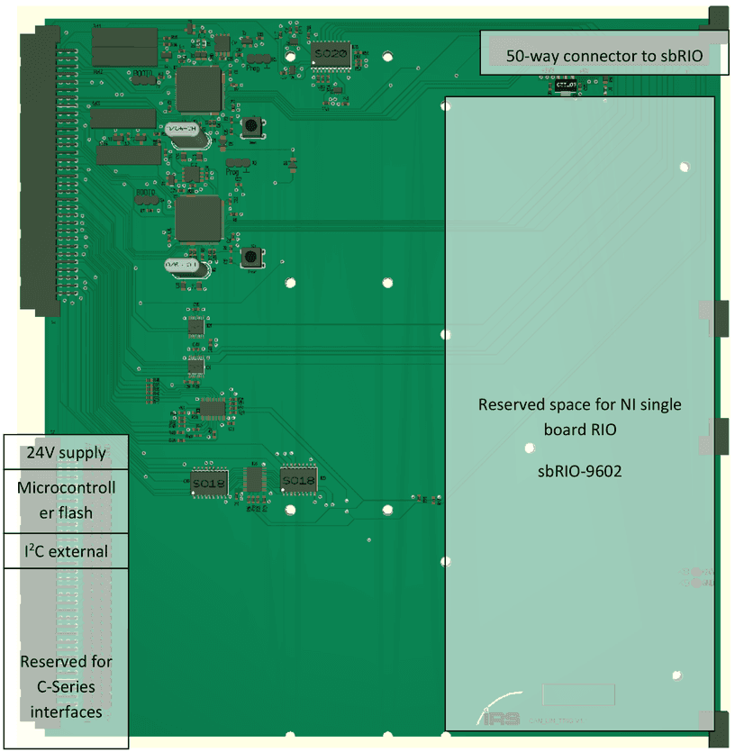
1.7.4Connection to sbRIO
The communication board is connected to sbRIO header P2 via a 50 way connector with the following pin assignments.
| Pin number P2 | Name | Description |
|---|---|---|
| 1 | GND | |
| 2 | SDA | I²C Bus data (port expanders) |
| 3 | SCL | I²C Bus clock (port expanders) |
| 4 | RX1 | LVDS RX1 (Interface to CMM) |
| 5 | RX2 | LVDS RX1 (Interface to CMM) |
| 6 | +5V | |
| 7 | TX2 | LVDS TX2 (Interface to CMM) |
| 8 | GND | |
| 9 | TX1 | LVDS TX1 (Interface to CMM) |
| 10 | +5V | |
| 11 | TX3 | LVDS TX3 (Interface to CMM) |
| 12 | GND | |
| 13 | SPI CS (2) | SPI BUS Chip select (Microcontroller 2) |
| 14 | GND | |
| 15 | SPI CLK (2) | SPI BUS Clock (Microcontroller 2) |
| 16 | GND | |
| 17 | SPI MISO (2) | SPI BUS MISO (Microcontroller 2) |
| 18 | GND | |
| 19 | SPI MOSI (2) | SPI BUS MOSI (Microcontroller 2) |
| 20 | GND | |
| 21 | EXT_I2C_SDA | SDA for external I2C |
| 22 | GPIO_2_1 | GPIO pin connection to microcontroller 2 |
| 23 | RIO HIGH-SPEED IN 1 | High-Speed buffered input |
| 24 | GND | |
| 25 | RIO HIGH-SPEED IN 2 | High-Speed buffered input |
| 26 | GND | |
| 27 | RIO HIGH-SPEED IN 3 | High-Speed buffered input |
| 28 | GND | |
| 29 | RIO HIGH-SPEED IN 4 | High-Speed buffered input |
| 30 | GND | |
| 31 | RIO HIGH-SPEED IN 5 | High-Speed buffered input |
| 32 | GND | |
| 33 | RIO HIGH-SPEED IN 6 | High-Speed buffered input |
| 34 | GND | |
| 35 | SPI CS (1) | SPI BUS Chip select (Microcontroller 1) |
| 36 | GND | |
| 37 | SPI CLK (1) | SPI BUS Clock (Microcontroller 1) |
| 38 | GND | |
| 39 | SPI MISO (1) | SPI BUS MISO (Microcontroller 1) |
| 40 | GND | |
| 41 | SPI MOSI (1) | SPI BUS MOSI (Microcontroller 1) |
| 42 | GND | |
| 43 | GPIO_1_1 | GPIO pin connection to microcontroller 1 |
| 44 | GND | |
| 45 | EXT_I2C_SCL | SCL for external I2C |
| 46 | GND | |
| 47 | PRG_RST_1 | Reset microcontroller 1 |
| 48 | GND | |
| 49 | PRG_RST_2 | Reset microcontroller 2 |
| 50 | GND |
1.7.5Pinning VG connector X1 (external signals)
| Pin | Signal | Pin | Signal | Pin | Signal |
|---|---|---|---|---|---|
| a1 | OPEN_COLL_16 | b1 | OPEN_COLL_15 | c1 | OPEN_COLL_14 |
| a2 | OPEN_COLL_13 | b2 | OPEN_COLL_12 | c2 | OPEN_COLL_11 |
| a3 | OPEN_COLL_10 | b3 | OPEN_COLL_09 | c3 | OPEN_COLL_08 |
| a4 | OPEN_COLL_07 | b4 | OPEN_COLL_06 | c4 | OPEN_COLL_05 |
| a5 | OPEN_COLL_04 | b5 | OPEN_COLL_03 | c5 | OPEN_COLL_02 |
| a6 | OPEN_COLL_01 | b6 | RIO_IN_05 | c6 | n.c. |
| a7 | Trig_16 | b7 | Trig_15 | c7 | Trig_14 |
| a8 | Trig_13 | b8 | Trig_12 | c8 | Trig_11 |
| a9 | Trig_10 | b9 | Trig_09 | c9 | Trig_08 |
| a10 | Trig_07 | b10 | Trig_06 | c10 | Trig_05 |
| a11 | Trig_04 | b11 | Trig_03 | c11 | Trig_02 |
| a12 | Trig_01 | b12 | LVDS_IN1- | c12 | LVDS_IN1+ |
| a13 | RIO_IN_01 | b13 | LVDS_IN2- | c13 | LVDS_IN2+ |
| a14 | RIO_IN_02 | b14 | LVDS_OUT1+ | c14 | LVDS_OUT1- |
| a15 | RIO_IN_03 | b15 | LVDS_OUT2+ | c15 | LVDS_OUT2- |
| a16 | RIO_IN_04 | b16 | LVDS_OUT3+ | c16 | LVDS_OUT3- |
| a17 | Serial_EN_10 | b17 | Serial_EN_09 | c17 | Serial_EN_08 |
| a18 | Serial_EN_07 | b18 | Serial_EN_06 | c18 | Serial_RX_09 |
| a19 | Serial_TX_08 | b19 | Serial_RX_08 | c19 | Serial_TX_09 |
| a20 | Serial_TX_06 | b20 | Serial_TX_07 | c20 | Serial_RX_07 |
| a21 | Serial_RX_06 | b21 | GPIO_2_4 | c21 | GPIO_2_3 |
| a22 | CAN_STDBY_2A | b22 | RIO_IN_06 | c22 | n.c. |
| a23 | CAN_ENABLE_2A | b23 | CAN_H_2B | c23 | CAN_L_2B |
| a24 | Serial_EN_05 | b24 | CAN_TX_2A | c24 | CAN_RX_2A |
| a25 | Serial_EN_02 | b25 | Serial_EN_03 | c25 | Serial_EN_04 |
| a26 | Serial_TX_05 | b26 | Serial_RX_05 | c26 | Serial_EN_01 |
| a27 | Serial_RX_03 | b27 | Serial_TX_04 | c27 | Serial_RX_04 |
| a28 | Serial_TX_02 | b28 | Serial_RX_02 | c28 | Serial_TX_03 |
| a29 | GPIO1_4 | b29 | Serial_TX_01 | c29 | Serial_RX_01 |
| a30 | Serial_RX_10 | b30 | Serial_TX_10 | c30 | GPIO_1_3 |
| a31 | CAN_H_1B | b31 | CAN_TX_1A | c31 | CAN_STDBY_1A |
| a32 | CAN_L_1B | b32 | CAN_RX_1A | c32 | CAN_ENABLE_1A |
1.7.6Pinning VG connector X2 (Power supply, Microcontroller Flashing, Reserved)
| Pin | Signal | Pin | Signal | Pin | Signal |
|---|---|---|---|---|---|
| B23 | SCL_Ext | C23 | SDA_Ext | ||
| C24 | µC1_Boot | ||||
| C25 | µC1_PRG_RST | ||||
| C26 | µC1_RxD | ||||
| C27 | µC1_TxD | ||||
| C28 | µC2_Boot | ||||
| C29 | µC2_PRG_RST | ||||
| C30 | µC2_RxD | ||||
| C31 | µC2_TxD | ||||
| a32 | +24V | B32 | GND | C32 | GND |
Pins C24 to C31 are used for Microcontroller flashing. This procedure is only performed at IRS. Do not connect any signals to these pins.
Pins B23 and C23 are used for connection of additional external modules via I²C. For using the I²C-interface refer to chapter 4.5.
The rest of the second VG connector X2 is almost entirely reserved for future use, especially for the wiring to additional C-series modules, which can be attached to the RIO via three SUB-D connectors and their inputs can be wired to the VG connector. All of the VG connector’s pins have been routed to three 32-way headers for this purpose.
1.7.7Communication line relations
Note, that there are two microcontrollers, which handle both 2 CAN interfaces and 5 serial interfaces, respectively. The following communication lines are assigned to the two microcontrollers according to the following table:
| µC1 | µC2 |
|---|---|
| CAN_1A | CAN_2A |
| CAN_1B | CAN_2B |
| Serial_01 | Serial_06 |
| Serial_02 | Serial_07 |
| Serial_03 | Serial_08 |
| Serial_04 | Serial_09 |
| Serial_05 | Serial_10 |
1.7.8CMM connection
For connection of the CMM, please refer to chapter 4.1.
1.8Analog input board 128x
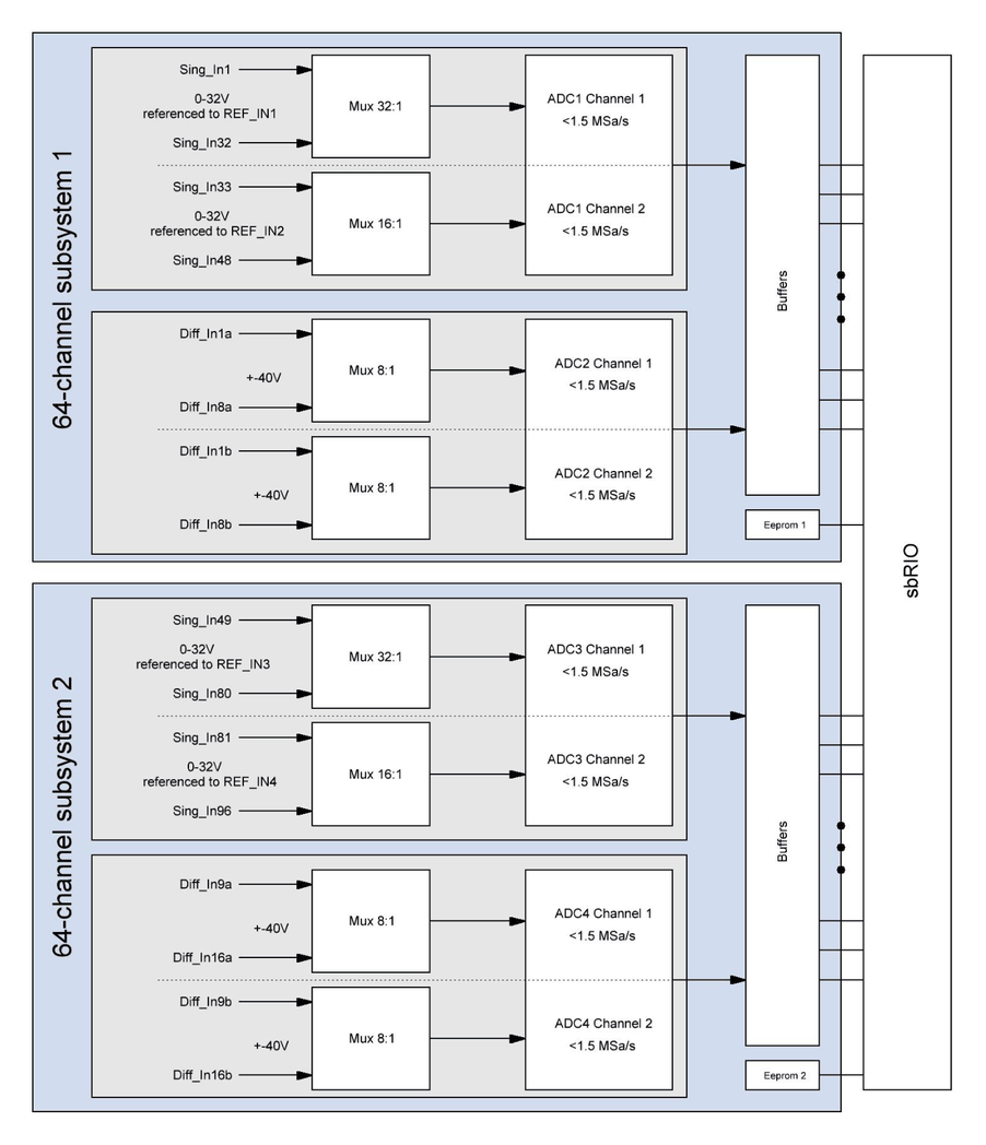
The analog input board provides 128 analog channels divided into two identical 64-channel subsystems with the following properties:
- 32 single-ended channels (external reference voltage 1), 0...32V @ 3 kS/s simultaneously
- 16 single-ended channels (external reference voltage 2) , 0...32V@ 6 kS/s simultaneously
- 16 differential channels, subdivided in simultaneously sampled groups of 8 channels each, -48...48V @ 150 kS/s in parallel.
To keep input currents as low as possible, no voltage divider was placed at the input of the single-ended channels. By connecting the signal directly to the non-inverting input of the input amplifier, very high input impedance is achieved. It should be noted that this open input causes the amplifiers to drift to the upper supply rail if no input voltage is connected. In this case, the ADCs return all ones (0x3FFF).
An EEPROM memory is provided that can be used to store calibration data, calibration values, an ID, the hardware revision and technical details (e.g. attenuation / gain of each channel).
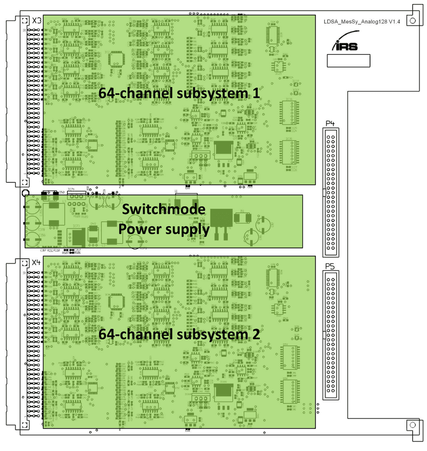
The analog input board is supplied by a single 24V DC supply as the whole measurement system. A switch mode power supply between the analog measurement subsystems generates positive and negative voltages and LDOs are used for linear regulation of these voltages to provide clean supply rails. Following figure illustrates the power supply unit of the analog input board.
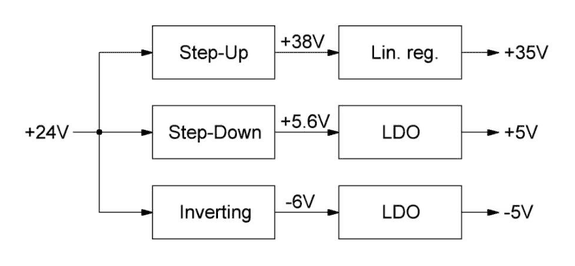
Soft start / power sequencing is included to reduce the inrush current at the moment the power supply is connected.
As shown in the following functional block diagram, the channels are multiplexed to ADCs with two channels each. 32 single-ended channels are handled by a 32:1 multiplexer with address lines ADR1_0 to ADR1_4, the remaining 16 single-ended channels are handled by a 16:1 multiplexer with address lines ADR2_0 to ADR2_3 and the differential channels are switched using two 8:1 multiplexers with shared address lines ADR3_0 to ADR3_2.
All address lines are buffered using high-speed CMOS buffers to reduce the load for the FPGA output drivers and to provide clean signals on the PCB.
1.8.1Block diagram
1.8.2Specifications
| Item | Min | Typical | Max | Unit |
|---|---|---|---|---|
| Supply current @24V | 400 | 440 | 500 | mA |
| Supply Voltage | 22 | 24 | 26 | VDC |
| Total number of channels | 128 | |||
| Number of single-ended channels | 96 | |||
| Number of differential channels | 32 |
All inputs are converted with a resolution of 14 bits.
The single-ended inputs can be sampled at a rate of 3kSa/s (channels 1-32 and 65-80) / 6kSa/s (channels 33-48 and 81 to 96) each, the differential inputs at more than 150kS/s.
If only one channel is measured, sampling rates of up to 1.2 MSa/s (possibly 1.5MSa) can be achieved.
The differential inputs are frequency-compensated for accurate waveform reproduction.
Specification of single-ended channels
| Item | Min | Typical | Max | Unit |
|---|---|---|---|---|
| Input voltage range (referenced to GND) | 0 | 32 | V | |
| Maximum sample rate (one channel) | 1.2 | MSa/s | ||
| Maximum sample rate (channel1-32, 49…80) | 3 | kSa/s | ||
| Maximum sample rate (channel 33-48, 81..96) | 6 | kSa/s | ||
| Voltage range of reference input vs. GND | -0.7 | 2.7 | V | |
| 3dB Bandwidth | 700 | kHz | ||
| Resolution | 14 | bit | ||
| Accuracy (not calibrated) | 1.0 | 2.0 | % Full scale | |
| Accuracy (after calibration) @ 5…30V | 0.1 | 0.3 | % of measured value | |
| Input Current @ 0 … 35V (current flows out of amplifier!) | 100 | 700 | nA | |
| Input resistance @ < 0V or >35V | 10 | kOhm |
Specification of differential channels
| Item | Min | Typical | Max | Unit |
|---|---|---|---|---|
| Input voltage range (differential) | -48 | 48 | V | |
| Input voltage range (common mode) | -60 | 60 | V | |
| Maximum sample rate (one channel) | 1.2 | MSa/s | ||
| Maximum sample rate (all diff. simultaneously) | 150 | kSa/s | ||
| 3dB Bandwidth | 1500 | kHz | ||
| Resolution | 14 | bit | ||
| Accuracy (not calibrated) | 2.0 | 4.0 | % Full scale | |
| Accuracy (after calibration) @ ±5…48V | 0.6 | 1.0 | % of measured value | |
| Input resistance (positive or negative input referenced to GND) | 400 | kOhm | ||
| Input resistance (positive and negative input differential) | 780 | kOhm |
1.8.3Layout
1.8.4Connection to sbRIO
The card is connected to sbRIO P4 and P5 via two 50 way connectors with the following pin assignment respectively
| Pin number P4 / P5 | Name | Description |
|---|---|---|
| 1…7 | n.c. | unused |
| 8 | GND | |
| 9 | ||
| 10 | ||
| 11 | SCL | Serial clock of on-board EEPROM |
| 12 | ||
| 13 | SDA | Serial data of on-board EEPROM |
| 14 | GND | |
| 15 | SDO2 | Serial Data of ADC2 |
| 16 | ||
| 17 | SDO | Serial data of ADC1 |
| 18 | GND | |
| 19 | ||
| 20 | GND | |
| 21 | Conv | Conversion start signal for ADCs |
| 22 | ||
| 23 | SCK | Serial clock for ADCs |
| 24 | ||
| 25 | ||
| 26 | ||
| 27 | Adr2_0 | Address line 1 of 16:1 multiplexer |
| 28 | ||
| 29 | Adr2_1 | Address line 2 of 16:1 multiplexer |
| 30 | ||
| 31 | Adr2_2 | Address line 3 of 16:1 multiplexer |
| 32 | ||
| 33 | Adr2_3 | Address line 4 of 16:1 multiplexer |
| 34 | ||
| 35 | Adr1_4 | Address line 5 of 32:1 multiplexer |
| 36 | ||
| 37 | Adr1_3 | Address line 4 of 32:1 multiplexer |
| 38 | ||
| 39 | Adr1_2 | Address line 3 of 32:1 multiplexer |
| 40 | ||
| 41 | Adr1_1 | Address line 2 of 32:1 multiplexer |
| 42 | ||
| 43 | Adr1_0 | Address line 1 of 32:1 multiplexer |
| 44 | ||
| 45 | Adr3_2 | Address line 3 of 8:1 multiplexers |
| 46 | GND | |
| 47 | Adr3_1 | Address line 2 of 8:1 multiplexers |
| 48 | ||
| 49 | Adr3_0 | Address line 1 of 8:1 multiplexers |
| 50 | GND |
1.8.5Pinning VG connector X3 (external signals Analog subsystem 1)
| Pin | Signal | Pin | Signal | Pin | Signal |
|---|---|---|---|---|---|
| a1 | Diff_In_3b+ | b1 | Diff_In_6a+ | c1 | Diff_In_1a+ |
| a2 | Diff_In_3b- | b2 | Diff_In_6a- | c2 | Diff_In_1a- |
| a3 | Diff_In_4b+ | b3 | Diff_In_7a+ | c3 | Diff_In_2a+ |
| a4 | Diff_In_4b- | b4 | Diff_In_7a- | c4 | Diff_In_2a- |
| a5 | Diff_In_5b+ | b5 | Diff_In_8a+ | c5 | Diff_In_3a+ |
| a6 | Diff_In_5b- | b6 | Diff_In_8a- | c6 | Diff_In_3a- |
| a7 | Diff_In_6b+ | b7 | Diff_In_1b+ | c7 | Diff_In_4a+ |
| a8 | Diff_In_6b- | b8 | Diff_In_1b- | c8 | Diff_In_4a- |
| a9 | Diff_In_7b+ | b9 | Diff_In_2b+ | c9 | Diff_In_5a+ |
| a10 | Diff_In_7b- | b10 | Diff_In_2b- | c10 | Diff_In_5a- |
| a11 | Diff_In_8b+ | b11 | GND | c11 | n.c. |
| a12 | Diff_In_8b- | b12 | GND | c12 | +24V |
| a13 | n.c. | b13 | n.c. | c13 | +24V |
| a14 | n.c. | b14 | n.c. | c14 | n.c. |
| a15 | REF_In_2 | b15 | n.c. | c15 | REF_In_1 |
| a16 | REF_In_2 | b16 | n.c. | c16 | REF_In_1 |
| a17 | Sing_In_48 | b17 | Sing_In_32 | c17 | Sing_In_16 |
| a18 | Sing_In_47 | b18 | Sing_In_31 | c18 | Sing_In_15 |
| a19 | Sing_In_46 | b19 | Sing_In_30 | c19 | Sing_In_14 |
| a20 | Sing_In_45 | b20 | Sing_In_29 | c20 | Sing_In_13 |
| a21 | Sing_In_44 | b21 | Sing_In_28 | c21 | Sing_In_12 |
| a22 | Sing_In_43 | b22 | Sing_In_27 | c22 | Sing_In_11 |
| a23 | Sing_In_42 | b23 | Sing_In_26 | c23 | Sing_In_10 |
| a24 | Sing_In_41 | b24 | Sing_In_25 | c24 | Sing_In_9 |
| a25 | Sing_In_40 | b25 | Sing_In_24 | c25 | Sing_In_8 |
| a26 | Sing_In_39 | b26 | Sing_In_23 | c26 | Sing_In_7 |
| a27 | Sing_In_38 | b27 | Sing_In_22 | c27 | Sing_In_6 |
| a28 | Sing_In_37 | b28 | Sing_In_21 | c28 | Sing_In_5 |
| a29 | Sing_In_36 | b29 | Sing_In_20 | c29 | Sing_In_4 |
| a30 | Sing_In_35 | b30 | Sing_In_19 | c30 | Sing_In_3 |
| a31 | Sing_In_34 | b31 | Sing_In_18 | c31 | Sing_In_2 |
| a32 | Sing_In_33 | b32 | Sing_In_17 | c32 | Sing_In_1 |
SING_In_1-SING_In_32 are referenced to REF_In_1, SING_In_33-SING_In_48 are referenced to REF_In_2.
1.8.6Pinning VG connector X4 (external signals Analog subsystem 2)
| Pin | Signal | Pin | Signal | Pin | Signal |
|---|---|---|---|---|---|
| a1 | Diff_In_11b+ | b1 | Diff_In_14a+ | c1 | Diff_In_9a+ |
| a2 | Diff_In_11b- | b2 | Diff_In_14a- | c2 | Diff_In_9a- |
| a3 | Diff_In_12b+ | b3 | Diff_In_15a+ | c3 | Diff_In_10a+ |
| a4 | Diff_In_12b- | b4 | Diff_In_15a- | c4 | Diff_In_10a- |
| a5 | Diff_In_13b+ | b5 | Diff_In_16a+ | c5 | Diff_In_11a+ |
| a6 | Diff_In_13b- | b6 | Diff_In_16a- | c6 | Diff_In_11a- |
| a7 | Diff_In_14b+ | b7 | Diff_In_9b+ | c7 | Diff_In_12a+ |
| a8 | Diff_In_14b- | b8 | Diff_In_9b- | c8 | Diff_In_12a- |
| a9 | Diff_In_15b+ | b9 | Diff_In_10b+ | c9 | Diff_In_13a+ |
| a10 | Diff_In_15b- | b10 | Diff_In_10b- | c10 | Diff_In_13a- |
| a11 | Diff_In_16b+ | b11 | GND | c11 | n.c. |
| a12 | Diff_In_16b- | b12 | GND | c12 | +24V |
| a13 | n.c. | b13 | n.c. | c13 | +24V |
| a14 | n.c. | b14 | n.c. | c14 | n.c. |
| a15 | REF_In_4 | b15 | n.c. | c15 | REF_In_3 |
| a16 | REF_In_4 | b16 | n.c. | c16 | REF_In_3 |
| a17 | Sing_In_96 | b17 | Sing_In_80 | c17 | Sing_In_64 |
| a18 | Sing_In_95 | b18 | Sing_In_79 | c18 | Sing_In_63 |
| a19 | Sing_In_94 | b19 | Sing_In_78 | c19 | Sing_In_62 |
| a20 | Sing_In_93 | b20 | Sing_In_77 | c20 | Sing_In_61 |
| a21 | Sing_In_92 | b21 | Sing_In_76 | c21 | Sing_In_60 |
| a22 | Sing_In_91 | b22 | Sing_In_75 | c22 | Sing_In_59 |
| a23 | Sing_In_90 | b23 | Sing_In_74 | c23 | Sing_In_58 |
| a24 | Sing_In_89 | b24 | Sing_In_73 | c24 | Sing_In_57 |
| a25 | Sing_In_88 | b25 | Sing_In_72 | c25 | Sing_In_56 |
| a26 | Sing_In_87 | b26 | Sing_In_71 | c26 | Sing_In_55 |
| a27 | Sing_In_86 | b27 | Sing_In_70 | c27 | Sing_In_54 |
| a28 | Sing_In_85 | b28 | Sing_In_69 | c28 | Sing_In_53 |
| a29 | Sing_In_84 | b29 | Sing_In_68 | c29 | Sing_In_52 |
| a30 | Sing_In_83 | b30 | Sing_In_67 | c30 | Sing_In_51 |
| a31 | Sing_In_82 | b31 | Sing_In_66 | c31 | Sing_In_50 |
| a32 | Sing_In_81 | b32 | Sing_In_65 | c32 | Sing_In_49 |
SING_In_1-SING_In_32 are referenced to REF_In_1, SING_In_33-SING_In_48 are referenced to REF_In_2.
The reference inputs are protected against signals of more than 2.7V above or 0.2V below ground but this range may only be exceeded for short periods of time!
The +24V supply will be connected to pins C12 & C13 of each VG-connector.
1.8.7Analog Accuracy
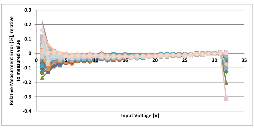
To obtain good accuracy a calibration procedure has to be performed. The gain and offset of every channel have to be determined after build-up. The gain and offset values are stored in the EEPROM of the analog input board. They are read at startup, and are used for every analog read out.
Single-ended channels
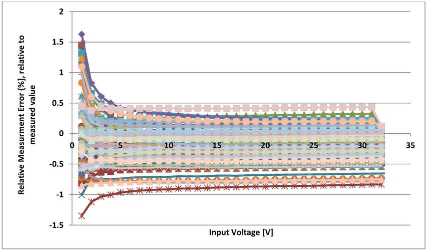
Following figure shows the typical accuracy of all 96 single ended channels not calibrated
Following figure shows the typical accuracy of all 96 single ended channels after calibration
Differential channels
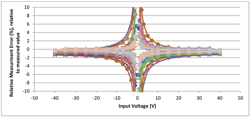
Following figure shows the typical accuracy of all 32 differential channels, not calibrated.
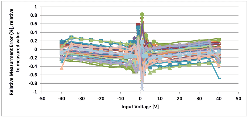
Following figure shows the typical accuracy of all 32 differential channels after calibration
1.9Digital Output board
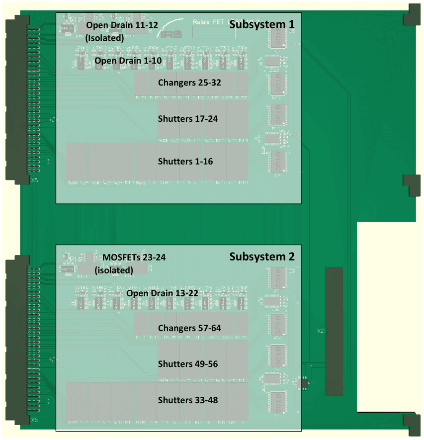
The digital output card provides 64 relays and 24 MOSFETs for general switching purposes. The relays are divided into 48 shutters and 16 changers. The MOSFETs are connected as open-drain low side switches and can handle up to 60V and 3A. However, the VG connector is only specified for 2A per pin so a current of 2A should not be exceeded. The overall current of all 10 FETs that switch to GND should be kept below 14A.
4 of the 24 transistors are galvanically isolated from the rest (and from each other).
The MOSFETs can each be switched directly from I/O pins of the sbRIO: a logical 0 turns the MOSFET on, a logical 1 off. Every MOSFET output may be used for fast switching applications as PWM.
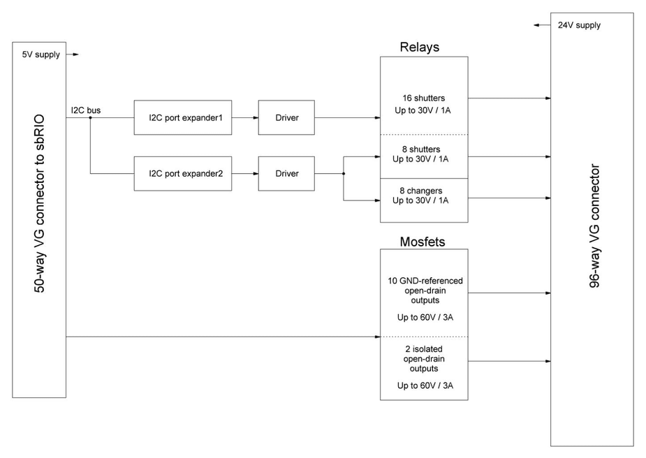
The relays have to be accessed through I²C port expanders. All port expanders are connected to the same I²C bus but have different addresses. The port expanders switch the relays with help of powerful driver ICs.
The Relais_FET_LDSA card consists of two identical subsystems. The MOSFET part and the port expanders of the card are powered from the sbRIO; the relays need an additional 24V supply on the VG connectors X5, X6.
1.9.1Block Diagram
A functional block diagram is shown below that illustrates how each of the subsystems works (i.e. one half of the total system).
1.9.2Specifications
| Item | Min | Typical | Max | Unit |
|---|---|---|---|---|
| Supply current @24V all Relays open | 4 | 7 | 20 | mA |
| Supply current @24V all Relays on | 600 | 700 | 800 | mA |
| Supply Voltage | 22 | 24 | 26 | VDC |
| Number of shutter relays | 48 | |||
| Number of changer relays | 16 | |||
| Number of open drain to System GND | 20 | |||
| Number of open drain isolated | 4 |
Open Drain MOSFET Outputs
| Item | Min | Typical | Max | Unit |
|---|---|---|---|---|
| voltage range | 60 | V | ||
| continuous current (limited by connector) | 0 | 2 | A | |
| RDS(on) @ | 60 | 100 | 150 | mOhm |
| Fall time tf | 0,5 | 1 | µs | |
| Rise time tr @ RPullup = 1 kOhm | 0,5 | 1 | µs |
Relays- Shutters
| Item | Min | Typical | Max | Unit |
|---|---|---|---|---|
| Switching Voltage | 60 | VDC or VACpeak | ||
| Switching current | 1.0 | A | ||
| Carry current | 1.25 | A | ||
| Contact resistance | 200 | mOhm | ||
| Life expectation @5 V / 10mA | 1000 | x106 cycles |
Relays- Changeover
| Item | Min | Typical | Max | Unit |
|---|---|---|---|---|
| Switching Voltage | 60 | VDC or VACpeak | ||
| Switching current | 1.0 | A | ||
| Carry current | 1.0 | A | ||
| Contact resistance @6V 10mA | 50 | mOhm | ||
| Life expectation @ no load | 1000 | x106 cycles | ||
| Life expectation @6 V / 100mA | 50 | x106 cycles |
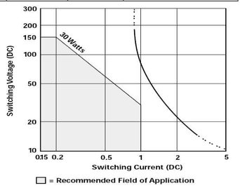
Following figure shows the maximum switching voltage, dependent on the switching current of the changeover relays.
1.9.3Layout
1.9.4Connection to sbRIO
The card is connected to sbRIO header P3 via a 50 way ribbon cable. The corresponding connector has the following pin assignments. Make sure the card is not connected to any other connector than P3 of the sbRIO!
| Pin number P3 | Name | Description |
|---|---|---|
| 1 | GND | |
| 2 | Open Drain 13 | |
| 3 | Open Drain 14 | |
| 4 | GND | |
| 5 | Open Drain 15 | |
| 6 | GND | |
| 7 | Open Drain 16 | |
| 8 | GND | |
| 9 | Open Drain 17 | |
| 10 | GND | |
| 11 | Open Drain 18 | |
| 12 | Open Drain 19 | |
| 13 | Open Drain 20 | |
| 14 | GND | |
| 15 | Open Drain 21 | |
| 16 | GND | |
| 17 | Open Drain 22 | |
| 18 | GND | |
| 19 | Open Drain 23 (isolated) | |
| 20 | GND | |
| 21 | Open Drain 24 (isolated) | |
| 22 | GND | |
| 23 | Open Drain 1 | |
| 24 | GND | |
| 25 | Open Drain 2 | |
| 26 | GND | |
| 27 | Open Drain 3 | |
| 28 | GND | |
| 29 | Open Drain 4 | |
| 30 | GND | |
| 31 | Open Drain 5 | |
| 32 | reserved | |
| 33 | Open Drain 6 | |
| 34 | GND | |
| 35 | Open Drain 7 | |
| 36 | GND | |
| 37 | Open Drain 8 | |
| 38 | GND | |
| 39 | SDA (I²C) | |
| 40 | GND | |
| 41 | SCL (I²C) | |
| 42 | GND | |
| 43 | Open Drain 9 | |
| 44 | +5V supply | |
| 45 | Open Drain 10 | |
| 46 | GND | |
| 47 | Open Drain 11 (isolated) | |
| 48 | +5V supply | |
| 49 | Open Drain 12 (isolated) | |
| 50 | GND |
1.9.5Pinning VG connector X5 (external signals digital subsystem 1)
| Pin | Signal | Pin | Signal | Pin | Signal |
|---|---|---|---|---|---|
| a1 | Rel1 (COM) | b1 | Rel2 (COM) | c1 | Rel3 (COM) |
| a2 | Rel1 (NO) | b2 | Rel2 (NO) | c2 | Rel3 (NO) |
| a3 | Rel4 (COM) | b3 | Rel5 (COM) | c3 | Rel6 (COM) |
| a4 | Rel4 (NO) | b4 | Rel5 (NO) | c4 | Rel6 (NO) |
| a5 | Rel7 (COM) | b5 | Rel8 (COM) | c5 | Rel9 (COM) |
| a6 | Rel7 (NO) | b6 | Rel8 (NO) | c6 | Rel9 (NO) |
| a7 | Rel10 (COM) | b7 | Rel11 (COM) | c7 | Rel12 (COM) |
| a8 | Rel10 (NO) | b8 | Rel11 (NO) | c8 | Rel12 (NO) |
| a9 | Rel13 (COM) | b9 | Rel14 (COM) | c9 | Rel15 (COM) |
| a10 | Rel13 (NO) | b10 | Rel14 (NO) | c10 | Rel15 (NO) |
| a11 | Rel16 (COM) | b11 | Rel17 (COM) | c11 | Rel18 (COM) |
| a12 | Rel16 (NO) | b12 | Rel17 (NO) | c12 | Rel18 (NO) |
| a13 | Rel19 (COM) | b13 | Rel20 (COM) | c13 | Rel21 (COM) |
| a14 | Rel19 (NO) | b14 | Rel20 (NO) | c14 | Rel21 (NO) |
| a15 | Rel22 (COM) | b15 | Rel23 (COM) | c15 | Rel24 (COM) |
| a16 | Rel22 (NO) | b16 | Rel23 (NO) | c16 | Rel24 (NO) |
| a17 | Rel25a (NC) | b17 | Rel26a (NC) | c17 | Rel27a (NC) |
| a18 | Rel25a (NO) | b18 | Rel26a (NO) | c18 | Rel27a (NO) |
| a19 | Rel25a (COM) | b19 | Rel26a (COM) | c19 | Rel27a (COM) |
| a20 | Rel28a (NC) | b20 | Rel29a (NC) | c20 | Rel30a (NC) |
| a21 | Rel28a (NO) | b21 | Rel29a (NO) | c21 | Rel30a (NO) |
| a22 | Rel28a (COM) | b22 | Rel29a (COM) | c22 | Rel30a (COM) |
| a23 | Rel31a (NC) | b23 | Rel32a (NC) | c23 | +24V |
| a24 | Rel31a (NO) | b24 | Rel32a (NO) | c24 | +24V |
| a25 | Rel31a (COM) | b25 | Rel32a (COM) | c25 | +24V |
| a26 | Open_Drain1 | b26 | Open_Drain8 | c26 | GND |
| a27 | Open_Drain2 | b27 | Open_Drain9 | c27 | GND |
| a28 | Open_Drain3 | b28 | Open_Drain10 | c28 | GND |
| a29 | Open_Drain4 | b29 | GND | c29 | Open_Drain11 |
| a30 | Open_Drain5 | b30 | GND | c30 | GND_ISO_11 |
| a31 | Open_Drain6 | b31 | GND | c31 | Open_Drain12 |
| a32 | Open_Drain7 | b32 | GND | c32 | GND_ISO_12 |
The open-drain outputs 1 to 10 all switch to GND while the isolated open-drain 11 and 12 switch to separate pins (GND_ISO_11 and GND_ISO_12).
1.9.6Pinning VG connector X6 (external signals digital subsystem 2)
| Pin | Signal | Pin | Signal | Pin | Signal |
|---|---|---|---|---|---|
| a1 | Rel33 (COM) | b1 | Rel34 (COM) | c1 | Rel35 (COM) |
| a2 | Rel33 (NO) | b2 | Rel34 (NO) | c2 | Rel35 (NO) |
| a3 | Rel36 (COM) | b3 | Rel37 (COM) | c3 | Rel38 (COM) |
| a4 | Rel36 (NO) | b4 | Rel37 (NO) | c4 | Rel38 (NO) |
| a5 | Rel39 (COM) | b5 | Rel40 (COM) | c5 | Rel41 (COM) |
| a6 | Rel39 (NO) | b6 | Rel40 (NO) | c6 | Rel41 (NO) |
| a7 | Rel42 (COM) | b7 | Rel43 (COM) | c7 | Rel44 (COM) |
| a8 | Rel42 (NO) | b8 | Rel43 (NO) | c8 | Rel44 (NO) |
| a9 | Rel45 (COM) | b9 | Rel46 (COM) | c9 | Rel47 (COM) |
| a10 | Rel45 (NO) | b10 | Rel46 (NO) | c10 | Rel47 (NO) |
| a11 | Rel48 (COM) | b11 | Rel49 (COM) | c11 | Rel50 (COM) |
| a12 | Rel48 (NO) | b12 | Rel49 (NO) | c12 | Rel50 (NO) |
| a13 | Rel51 (COM) | b13 | Rel52 (COM) | c13 | Rel53 (COM) |
| a14 | Rel51 (NO) | b14 | Rel52 (NO) | c14 | Rel53 (NO) |
| a15 | Rel54 (COM) | b15 | Rel55 (COM) | c15 | Rel56 (COM) |
| a16 | Rel54 (NO) | b16 | Rel55 (NO) | c16 | Rel56 (NO) |
| a17 | Rel57a (NC) | b17 | Rel58a (NC) | c17 | Rel59a (NC) |
| a18 | Rel57a (NO) | b18 | Rel58a (NO) | c18 | Rel59a (NO) |
| a19 | Rel57a (COM) | b19 | Rel58a (COM) | c19 | Rel59a (COM) |
| a20 | Rel60a (NC) | b20 | Rel61a (NC) | c20 | Rel62a (NC) |
| a21 | Rel60a (NO) | b21 | Rel61a (NO) | c21 | Rel62a (NO) |
| a22 | Rel60a (COM) | b22 | Rel61a (COM) | c22 | Rel62a (COM) |
| a23 | Rel63a (NC) | b23 | Rel64a (NC) | c23 | +24V |
| a24 | Rel63a (NO) | b24 | Rel64a (NO) | c24 | +24V |
| a25 | Rel63a (COM) | b25 | Rel64a (COM) | c25 | +24V |
| a26 | Open_Drain13 | b26 | Open_Drain20 | c26 | GND |
| a27 | Open_Drain14 | b27 | Open_Drain21 | c27 | GND |
| a28 | Open_Drain15 | b28 | Open_Drain22 | c28 | GND |
| a29 | Open_Drain16 | b29 | GND | c29 | Open_Drain23 |
| a30 | Open_Drain17 | b30 | GND | c30 | GND_ISO_23 |
| a31 | Open_Drain18 | b31 | GND | c31 | Open_Drain24 |
| a32 | Open_Drain19 | b32 | GND | c32 | GND_ISO_24 |
The open-drain outputs 12 to 22 all switch to GND while the isolated open-drain 23 and 24 switch to separate pins (GND_ISO_23 and GND_ISO_24).
1.9.7PWM timing with MOSFETs
All Open Drain outputs, including the isolated ones, can be used for PWM generation.
The following figure shows the typical timing behaviour of a MOSFET output with an external pull-up of 1 kOhm connected
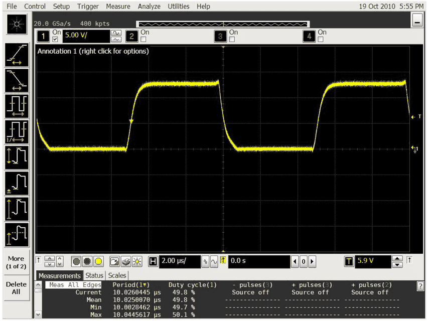
Note that with pull-up resistors of higher resistance, higher rise times will occur. The fall time is quite independent of the pull-up resistor size.
The sbRIO-SW uses a timing resolution of 1µs. If necessary, the resolution can be adjusted up to 25ns. But note, that this would reduce maximum period of signal generation.
Documents and downloads
Further documents and files for your IRS product are available on myIRS.